
Photographs (about 100 KBytes each, click on the image for a larger view) |
|
 |
|
 |
|
 |
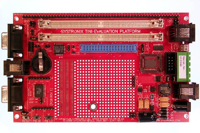
STEP.IR without TINI module installed. |
 |
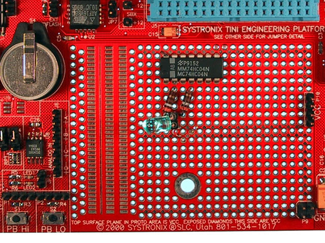
Close up of STEP.IR IrDA components. |
Photographs (about 100 KBytes each, click on the image for a larger view) |
|
|
|
|
|
|
|
|
|
STEP.IR without TINI module installed. |
|
|
Close up of STEP.IR IrDA components. |